ELEC2311 · UWA · 2025

VHDL Digital
System Design

DE10-Lite FPGA · Quartus Prime · ModelSim · Intel MAX 10
✓ Complete VHDL DE10-Lite FPGA Quartus Prime

Second-year digital design unit at UWA. Designed and synthesised a series of VHDL modules on the Intel DE10-Lite FPGA — D-latches, flip-flops, 7-segment decoders, 8-bit counters, and a clock divider. The D-latch and the clock divider started from files supplied by the unit; the flip-flops and their testbenches, the 7-segment decoder, the counter and the full adder are my own. Simulated in ModelSim and tested on the board.

Result Designed and synthesised 6 digital circuits on Intel DE10-Lite FPGA — D-latch, flip-flop, 7-segment decoder, 8-bit counter, clock divider, and full adder — simulated in ModelSim and tested on the board.
Platform
DE10-Lite
Intel MAX 10 FPGA (10M50DAF484C7G)
Language
VHDL
IEEE 1076 standard
Synthesis
Quartus
Quartus Prime Lite
Simulation
ModelSim
Testbench-driven
At a Glance
TypeUniversity unit: ELEC2311 Digital System Design, UWA
Year2025
My workLab and mock-test designs; two starting files supplied by the unit
SkillsVHDL · testbenches · synthesis · FPGA pin mapping
ToolsQuartus Prime · ModelSim · DE10-Lite
StatusComplete

ELEC2311 introduces digital design as a hardware description problem, not just circuit drawing. VHDL is used to describe hardware behaviour which is then synthesised into gate-level netlists by Quartus Prime and programmed onto the DE10-Lite's MAX 10 FPGA. The board runs a 50 MHz onboard clock and exposes switches, push buttons, LEDs, and HEX displays for I/O.

The unit covered three modelling styles — dataflow (concurrent signal assignments), behavioural (processes with sequential logic), and structural (component instantiation). Designs were checked with ModelSim testbenches before being loaded onto the board.

▣
D-Latch (positive level)
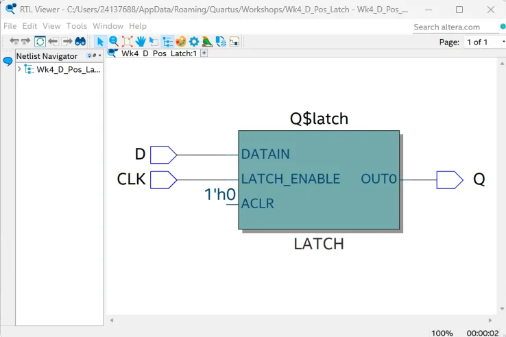
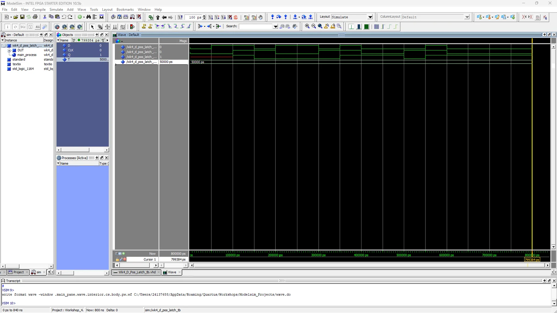
Level-sensitive latch — transparent when CLK=1, holds when CLK=0. Written as a behavioural process with an intentional incomplete if-else to infer latch behaviour. Starting file and testbench supplied in Lab 3; RTL checked in the Quartus viewer.
◉
D Flip-Flop with Testbench
Edge-triggered D flip-flop with full testbench. The testbench drives D and CLK with a 20 ns clock period (50 MHz); Q was checked on the ModelSim waveform at each rising edge.
▦
7-Segment Decoder
4-bit binary input → 7-segment HEX0 output covering 0–F. Implemented as a case statement in a process(all) block targeting the DE10-Lite's active-low segment driver. Switch inputs mapped to LEDR simultaneously.
⌁
8-bit Synchronous Counter
Structural up counter built from 8 T flip-flops instantiated in a generate loop, clocked from the 50 MHz board clock with asynchronous active-low clear. Each flip-flop's T input is gated by Enable and every lower-order bit, so all 8 stages toggle on the same clock edge.
∿
Clock Divider to 1 Hz
Divides the 50 MHz DE10-Lite clock down to 1 Hz using a parameterised counter. The generic Freq_in allows the divisor to be changed at elaboration time without editing the architecture. Supplied by the unit in Lab 4; I used it to drive visible LED blink rates.
+
1-bit Full Adder
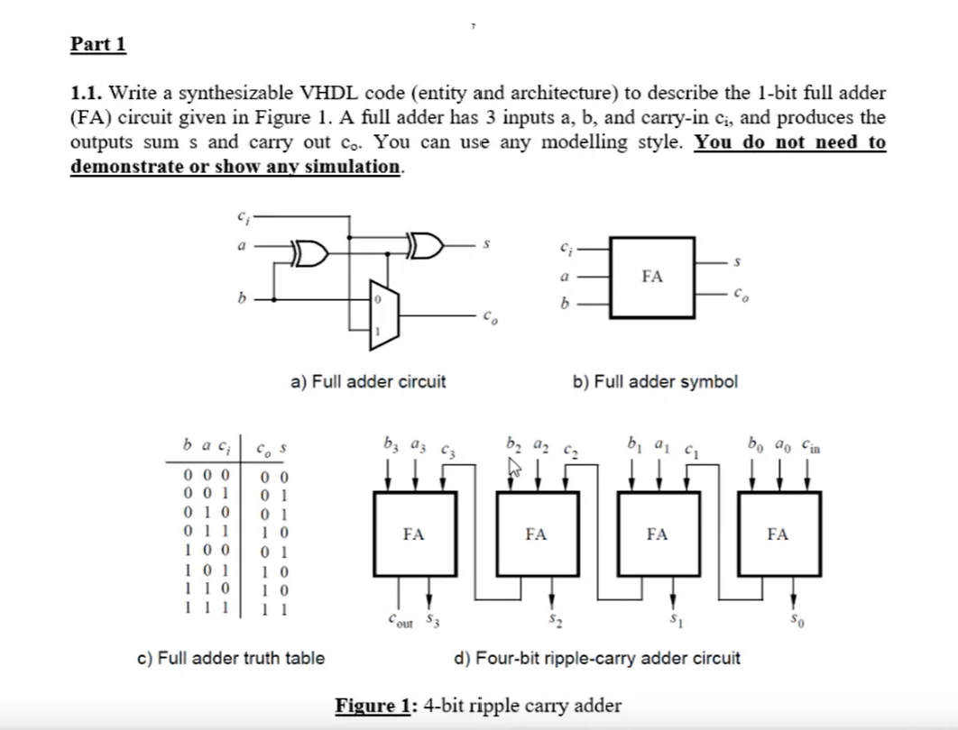
1-bit full adder with carry-in and carry-out, written as a behavioural process. A concurrent XOR (a⊕b) computes an intermediate select signal that muxes the carry-out between carry-in and b; the sum is computed inside the same process. Written for the mid-unit mock test.

Code

Two representative designs — the 7-segment decoder (combinational dataflow/behavioural) and the clock divider (sequential behavioural with a generic, supplied by the unit). Both target the DE10-Lite's standard port names directly.

7_SEGMENT_DISPLAY.vhd DE10-Lite · Combinational
library IEEE;
use IEEE.STD_LOGIC_1164.ALL;

entity top is
  port (
    CLOCK_50 : in  STD_LOGIC;
    SW       : in  STD_LOGIC_VECTOR(9 downto 0);
    LEDR     : out STD_LOGIC_VECTOR(9 downto 0);
    HEX0     : out STD_LOGIC_VECTOR(6 downto 0)
  );
end entity;

architecture rtl of top is
begin
  LEDR(3 downto 0) <= SW(3 downto 0);  -- mirror switch inputs to LEDs

  process(all)
  begin
    case SW(3 downto 0) is
      when "0000" => HEX0 <= "1000000"; -- 0
      when "0001" => HEX0 <= "1111001"; -- 1
      when "0010" => HEX0 <= "0100100"; -- 2
      when "0011" => HEX0 <= "0110000"; -- 3
      -- ... 0100 through 1111 (A–F) ...
      when others => HEX0 <= "0001110"; -- F
    end case;
  end process;
end architecture;
Clk_divider_to_1Hz.vhd DE10-Lite · Sequential · 50 MHz → 1 Hz
entity Clk_divider_to_1Hz is
  generic(
    Freq_in : integer := 50000000  -- 50 MHz onboard clock
  );
  port (
    clk_in  : in  STD_LOGIC;
    reset   : in  STD_LOGIC;
    clk_out : out STD_LOGIC
  );
end Clk_divider_to_1Hz;

architecture Behav of Clk_divider_to_1Hz is
  signal temp    : STD_LOGIC;
  signal counter : integer;
  constant N     : integer := 2;  -- f_out = N/2 Hz
begin
  frequency_divider: process(reset, clk_in)
  begin
    if (reset = '1') then
      temp    <= '0';
      counter <= 0;
    elsif rising_edge(clk_in) then
      if (counter = Freq_in/N) then
        temp    <= NOT(temp);  -- toggle output
        counter <= 0;
      else
        counter <= counter + 1;
      end if;
    end if;
  end process;

  clk_out <= temp;
end Behav;

Tools & Flow

Quartus Prime — Synthesis
Target deviceIntel MAX 10, 10M50DAF484C7G (DE10-Lite)
Entry methodVHDL source files
VerificationRTL Viewer — netlist inspection
Pin assignmentDE10-Lite Qsf file (standard)
ProgrammingUSB-Blaster → .sof file
ModelSim — Simulation
Testbench styleSeparate _tb entity
Clock period20 ns (50 MHz sim clock)
VerificationWaveform visual inspection
DUT instantiationPORT MAP in testbench
StimulusSignal assignments + wait statements

The design flow for every module was: write VHDL source → compile in Quartus and check for syntax errors → run synthesis and inspect the RTL Viewer to confirm the inferred hardware matches intent → write a testbench → simulate in ModelSim and check waveforms → if simulation passes, program the DE10-Lite and verify on hardware.

The key insight from this unit: VHDL describes hardware that runs concurrently. A process does not execute sequentially the way a C function does — all processes in an architecture run in parallel, triggered by their sensitivity lists. Getting this mental model right early was the most important thing the unit taught.

Simulation & Synthesis
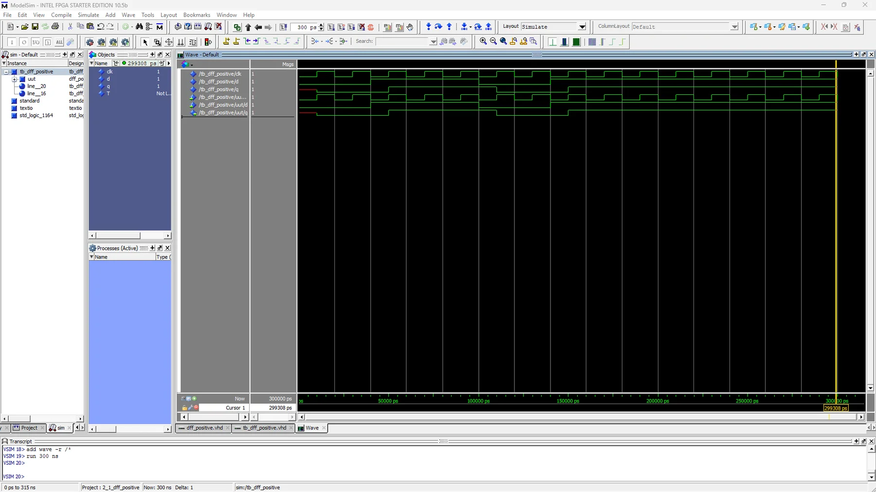
ModelSim waveform — D flip-flop testbench
ModelSim — D flip-flop testbench waveform
ModelSim waveform
RTL viewer
ModelSim sim
Mock test circuit
Key Concepts Applied
Concurrent vs sequentialSignal assignments outside process = concurrent; inside = sequential
Latch inferenceIncomplete if-else in a clocked process → Quartus infers a latch
rising_edge()Correct way to describe synchronous logic (not clk'event)
Generic constantsFreq_in generic lets clock divider be reused at any frequency
Sensitivity listprocess(all) catches all signals — avoids simulation/synthesis mismatch
PORT MAPTestbench instantiates DUT with named association — clearer than positional
← RetroDS v2 ⌂ Portfolio ESP32-S3 Dev Board →