Engineering Design Portfolio — Embedded Systems

RetroDS — ESP32 NES
Handheld Console

Hand-Soldered Perfboard Build  /  Arduino Framework  /  Feb 2026 → PCB shipped as v2
ESP32-WROOM-32E · 240 MHz ST7789 · 240×240 IPS Audio · PCB Build MicroSD · FAT32
8× GPIO Buttons LiPo · USB-C Charge Prototype ✓ · PCB → v2 KiCad PCB · Shipped as v2
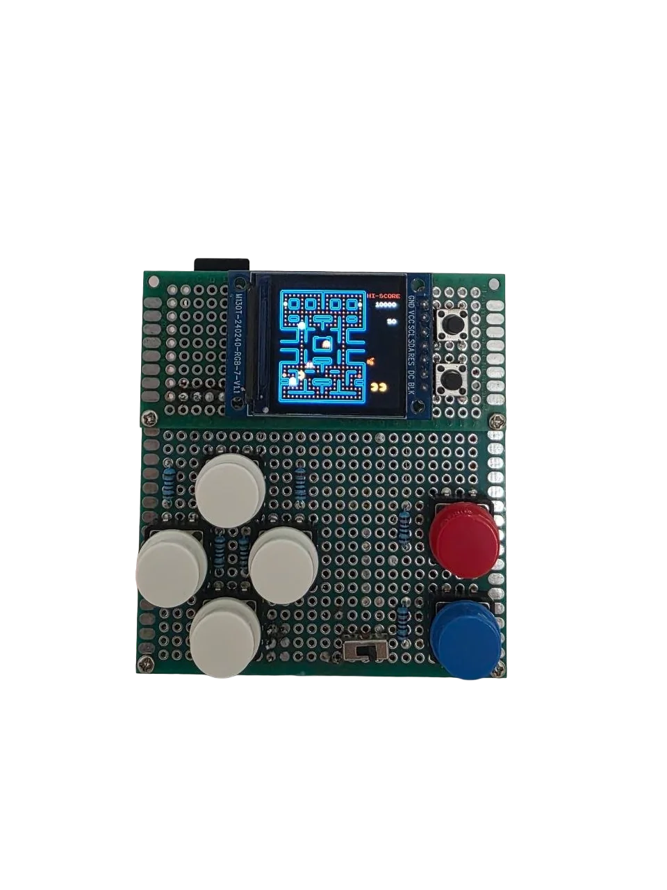
Result Hand-built a working portable NES emulator on perfboard — 6502 CPU core, PPU rendering, audio output, and controller input running on a 240 MHz ESP32-WROOM. Prototype plays ROM images without issues.
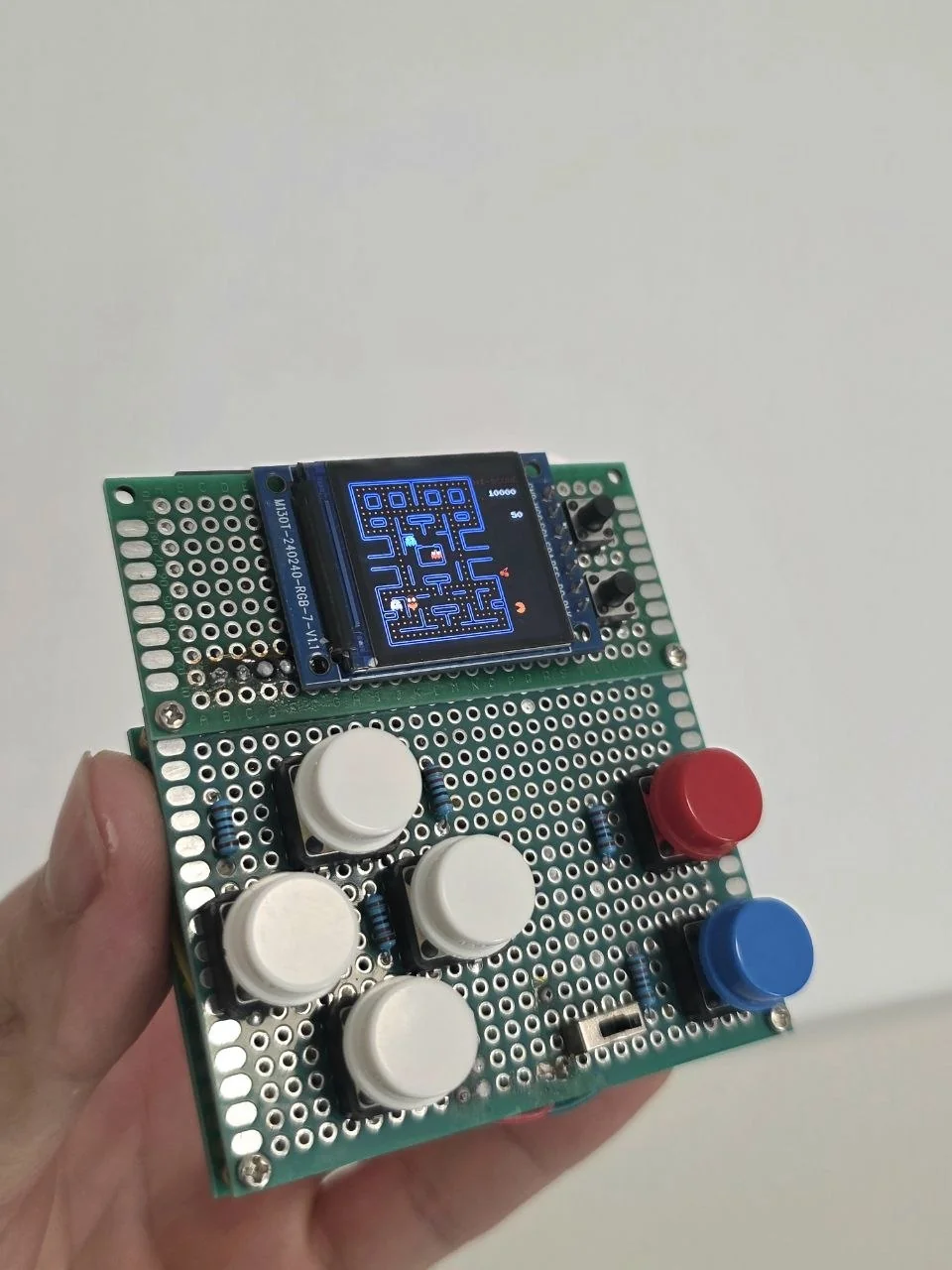
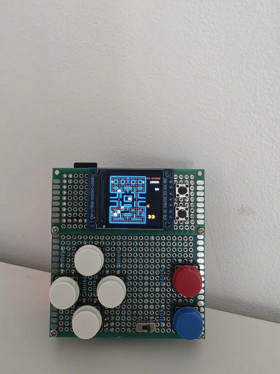
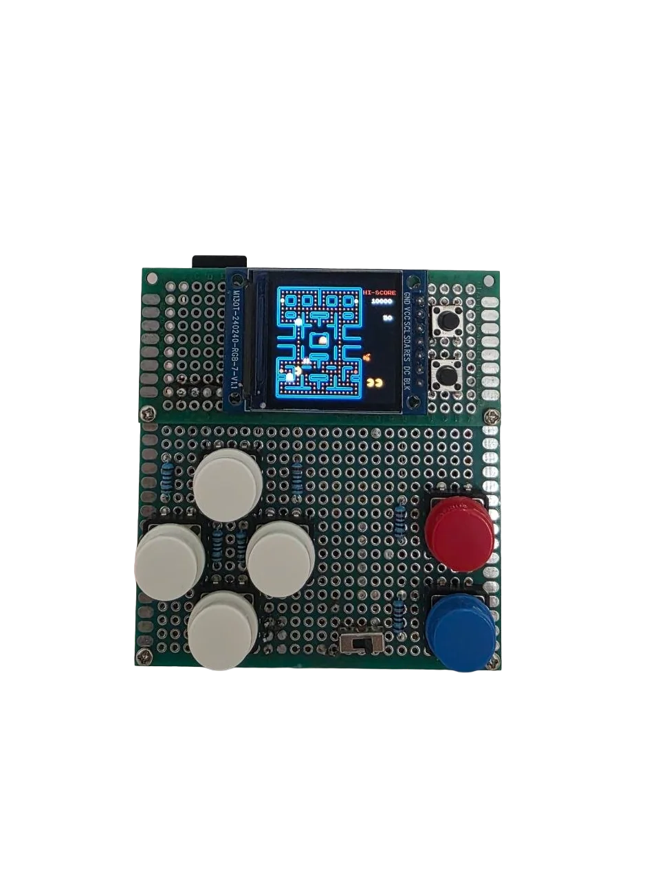
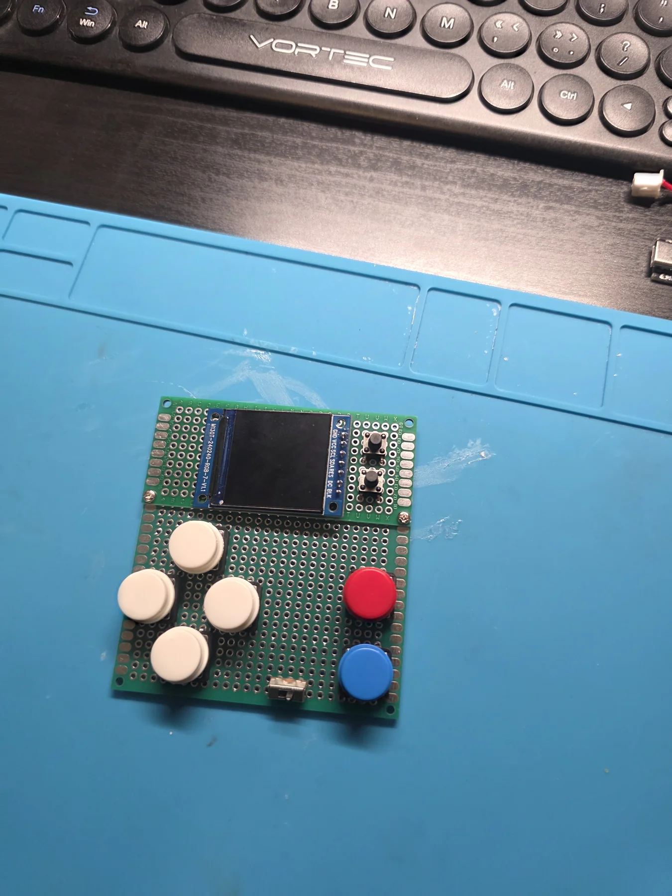
RetroDS handheld console — completed perfboard build running Pac-Man

This started as "how hard can an NES emulator be" and turned into a three-month project. The emulator core came from the open-source NESCAT project — the hard part was getting it running on my own hardware. Lost about a week to a display corruption bug that turned out to be my SPI clock running 3 MHz too fast for my specific display module. Built on perfboard first because I didn't trust my PCB skills yet — and I'm glad I did. Version 2 takes it to a custom 4-layer PCB — built, working, and documented.

RetroDS NES Emulator — real build photo
RetroDS — Perfboard Build, April 2026
Build photo 1
Running ROM
Display in action
Game running
Display close-up
Wiring detail
Handheld build
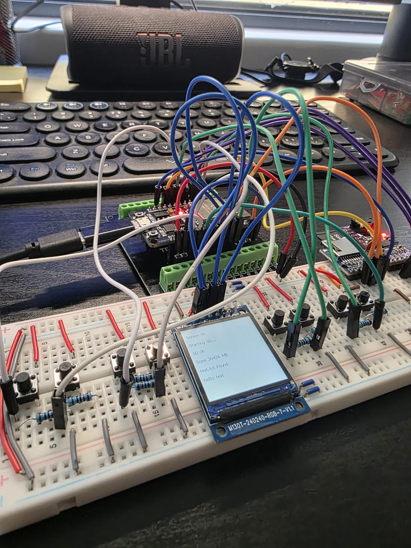
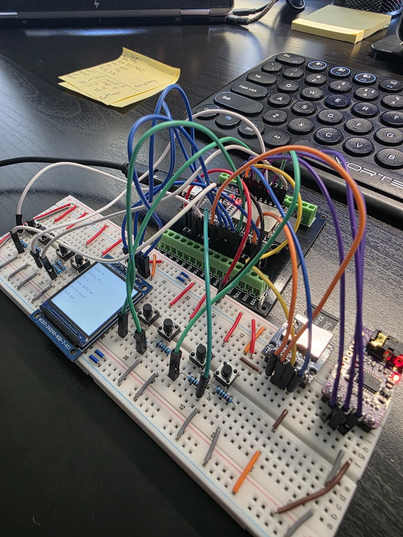
Breadboard prototype
Early layout
Prototyping
Wiring detail
Breadboard setup
Component assembly
Late stage wiring
Key Components
ESP32-WROOM
ST7789 IPS
MicroSD
MAX98357A
LiPo + USB-C
8 Buttons
Build Progress
✓
Research
✓
Perfboard
✓
Firmware
✓
ROM Loading
→
PCB Design
Assembly
What I Learned
  • My ST7789 display refused to work above 27 MHz SPI even though the datasheet claims 80 MHz. Different display, different silicon, different actual limits. Always test your specific module, not the spec sheet.
  • Perfboard cold joints are invisible and crash under vibration, not under button presses — so I spent a week thinking my firmware had a bug. Good flux and patience is the fix. And a magnifying glass.
240 px
Display Resolution
27 MHz
SPI Clock
512 KB
Max ROM Size
8 buttons
Input Buttons
Build log, firmware details, and PCB plans below ↓
01

Project Overview

CPU Speed
240
MHz dual-core ESP32
Display
240×240
ST7789 IPS @ 27 MHz SPI
Audio
24
kHz I2S — firmware ready, wired on PCB
Mapper Support
40+
NROM, MMC1–5, UNROM, VRC & more
At a Glance
TypePersonal project
My roleHand-soldered build, wiring, display and SD bring-up, port to my hardware
TimelineFeb 2026 → continued as v2 PCB
SkillsPerfboard prototyping · SPI displays · fault-finding
ToolsArduino IDE · multimeter · soldering iron
StatusPrototype working · replaced by the v2 PCB
Built On (Credits)
Emulator coreNESCAT by Nathalis (GPL-3.0)
Display libraryTFT_eSPI
My workHardware build and the port to it

RetroDS is a battery-powered handheld NES emulator I designed and built on an ESP32-WROOM-32E. The firmware is based on the open-source NESCAT emulator by Nathalis (GPL-3.0), which provides the 6502 CPU emulator, PPU graphics renderer and APU audio; I adapted it to my hardware. Game output goes to a 240×240 IPS TFT display. ROMs are loaded from a MicroSD card at runtime. Audio was written in firmware but not wired into the prototype — it is implemented on the PCB.

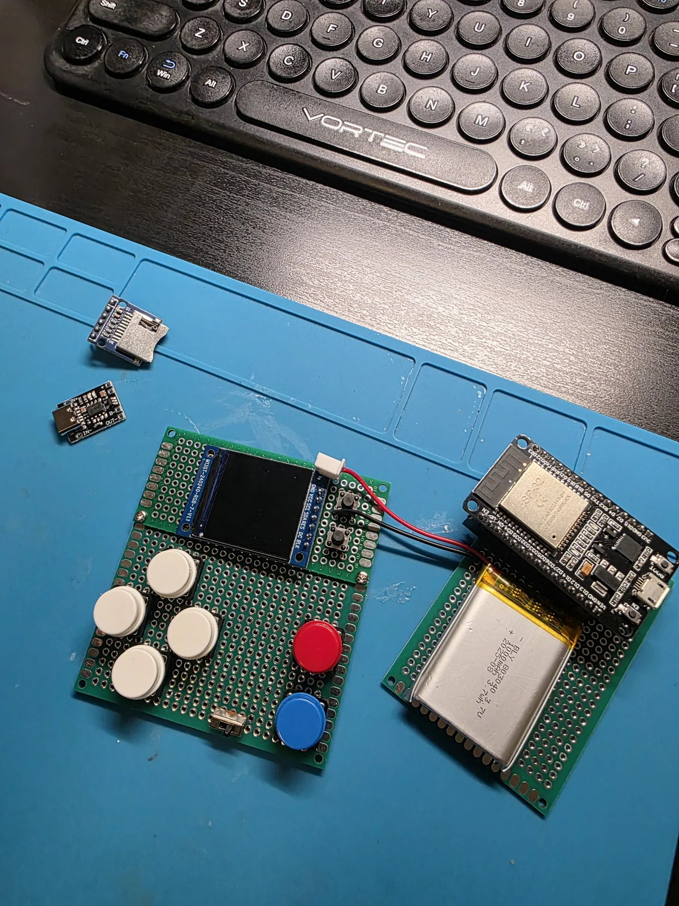
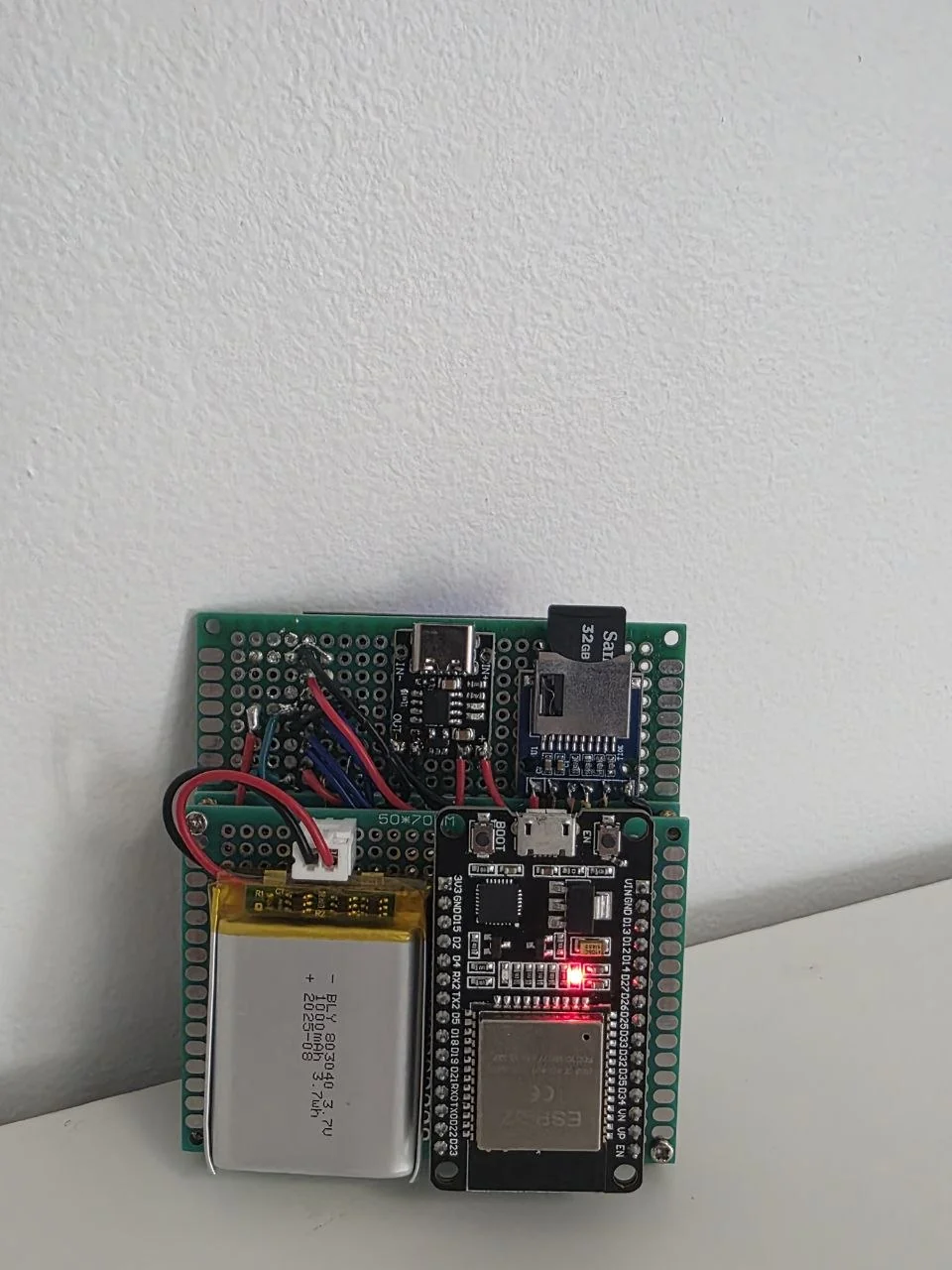
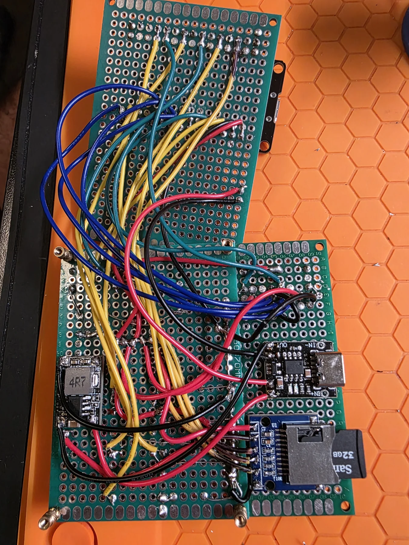
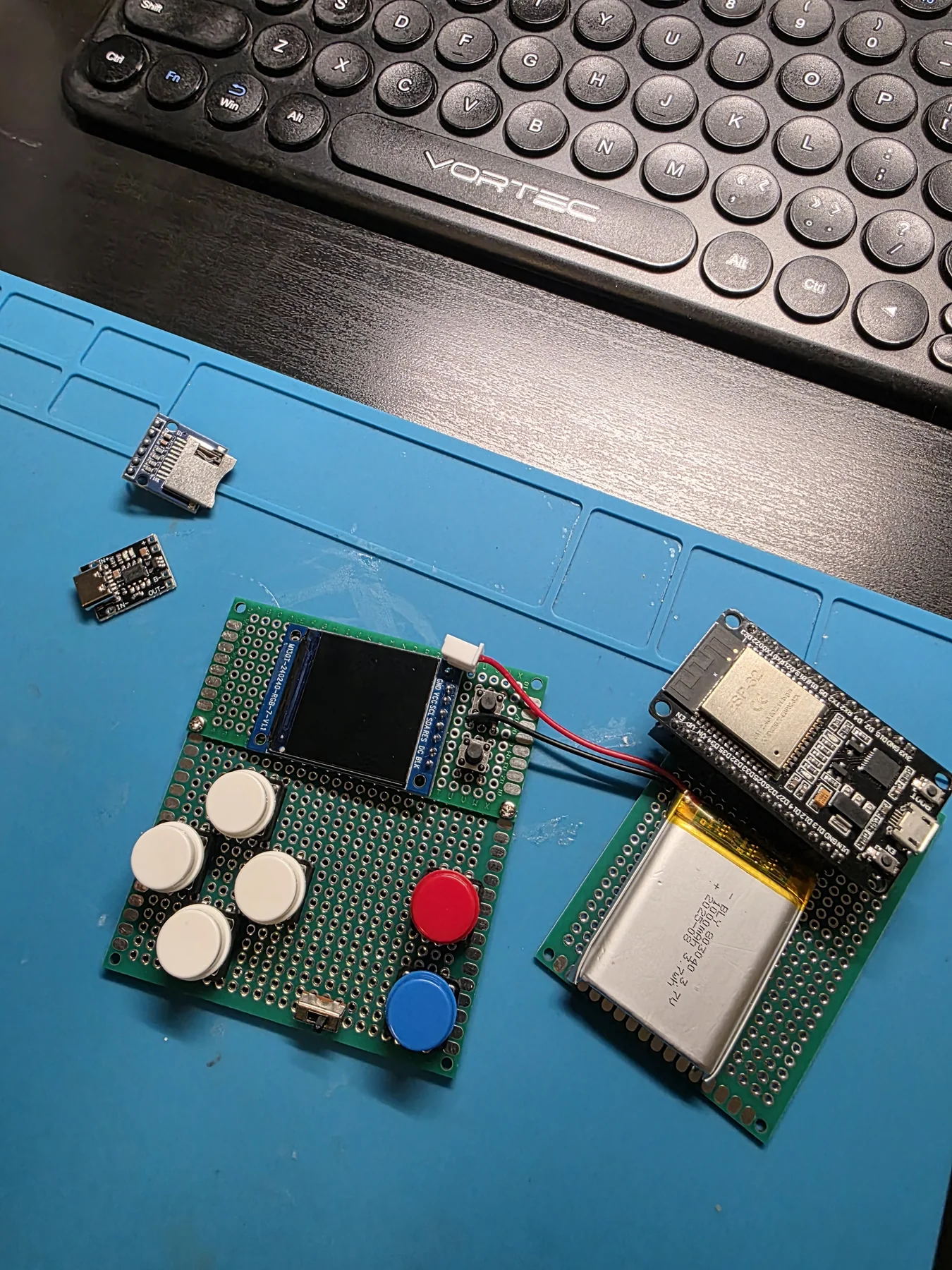
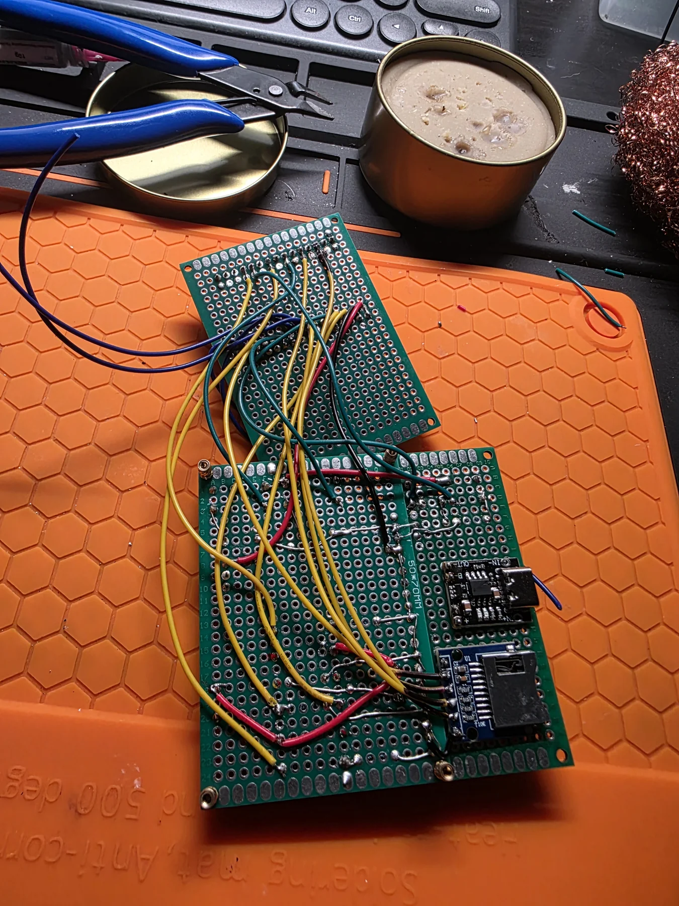
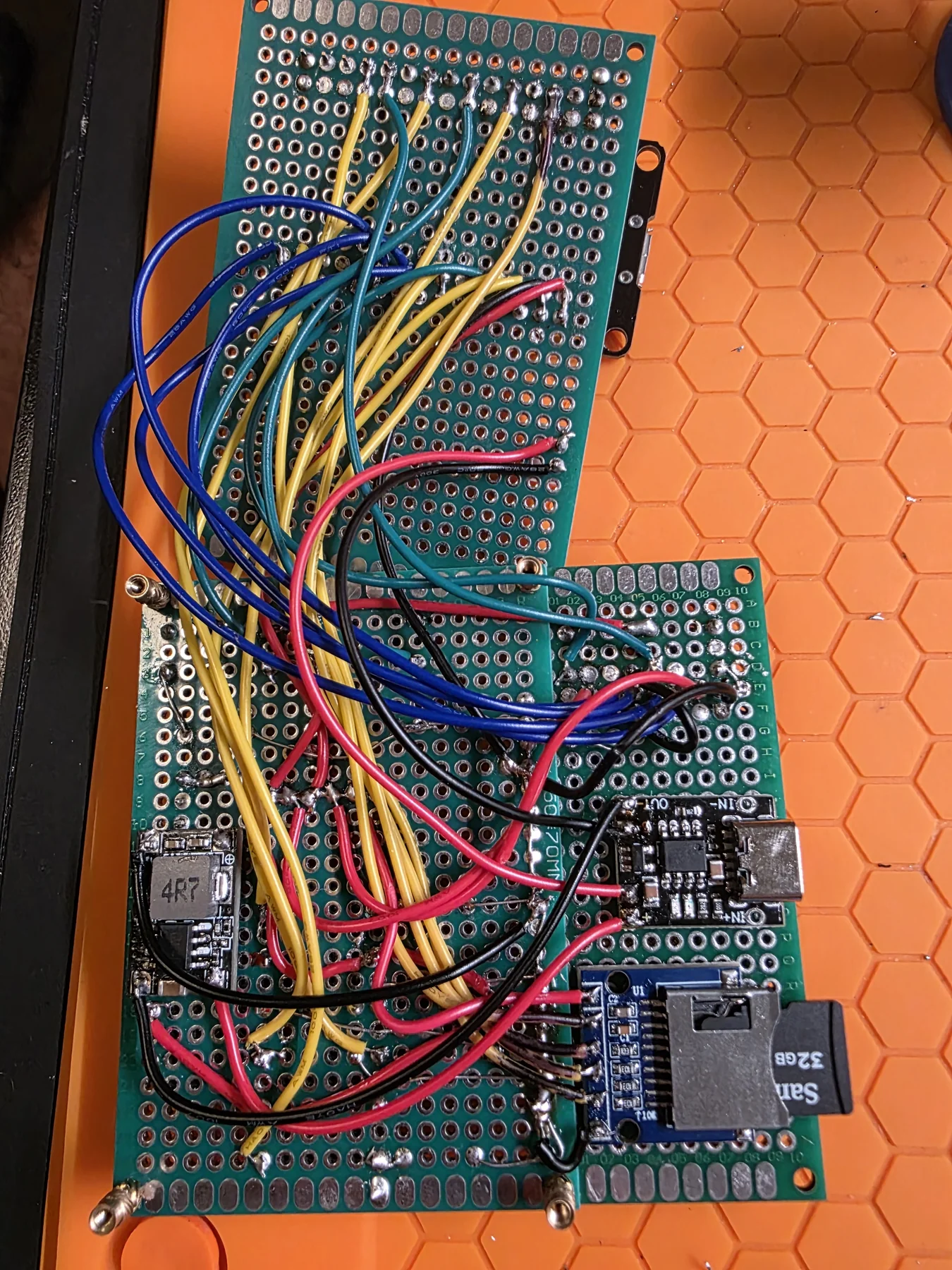
The build progressed from a breadboard prototype to a hand-soldered perfboard console. The front board carries the ST7789 display, D-pad, and action buttons; the back carries the ESP32, MicroSD breakout, and power management ICs. That perfboard stack has since been consolidated onto a single custom 4-layer KiCad PCB, shipped as RetroDS v2.
02

Components

All components are off-the-shelf breakout modules wired onto perfboard. The ESP32 operates at 3.3 V logic throughout, with the power management chain stepping up from the LiPo cell and regulating down to logic level.

Ref Component Part / Value Interface Notes
U1 Microcontroller ESP32-WROOM-32E — 240 MHz dual-core Xtensa LX6, 4 MB Flash, 520 kB SRAM
U2 Display ST7789 1.3″ IPS TFT 240×240 SPI @ 27 MHz TFT_eSPI library — requires User_Setup.h edit (Section 05)
U3 Audio Amplifier MAX98357A — PCB only I2S Class D amp + DAC in one chip — not in prototype; drives speaker directly on PCB build
U4 SD Card Module MicroSD SPI Breakout Soft-SPI FAT32, tested up to 30 GB; software SPI avoids display bus conflict
U5 Power Management IC IP5306 I²C 5 V boost converter with USB-C charge indicator LEDs
U6 Charge Controller TP4056 USB-C Module — 1 A LiPo charge controller, over-current and over-voltage protection
BT1 Battery LiPo 3.7 V cell — Rechargeable lithium polymer; capacity sized for portable use
SW1–8 Input Buttons Tactile push switches ×8 GPIO pull-up D-pad (4) + A/B + START/SELECT; internal pull-ups, software debounce
C1–C4 Decoupling Capacitors 100 nF + 10 μF — Per VDD rail, placed adjacent to MCU power pins
03

Hardware Architecture

Five subsystems are interconnected on perfboard via point-to-point soldered wiring. The hardware SPI bus is reserved exclusively for the display — CS is tied permanently low, so no other device can share it. The SD card uses a separate set of GPIO pins running software SPI. All subsystems were validated on breadboard before final perfboard assembly.

SubsystemComponentInterfaceKey Notes
MicrocontrollerESP32-WROOM-32E—240 MHz dual-core, 4 MB Flash, 520 kB SRAM
DisplayST7789 1.3″ IPS 240×240HW SPI @ 27 MHzCS tied low (always active); pins defined in TFT_eSPI User_Setup.h
AudioNot in prototype — PCB onlyI2SFirmware written and ready; MAX98357A amp wired on PCB build
StorageMicroSD BreakoutSoft-SPIMOSI GPIO 17 · MISO GPIO 13 · SCK GPIO 14 · CS GPIO 22
User Input8× Tactile ButtonsGPIO Pull-upD-pad (4) + A/B + Start/Select — internal pull-ups enabled
PowerLiPo 3.7 V + IP5306—USB-C charge via TP4056 · 5 V boost · 3.3 V regulated logic
Decoupling100 nF + 10 μF—Per VDD rail, placed adjacent to MCU power pins
Display Pins
TFT MOSIGPIO 23
TFT SCLKGPIO 18
TFT DCGPIO 5
TFT RSTGPIO 19
TFT CS–1 (always active)
Storage & Input Pins
SD MOSI / MISO / SCK / CS17 / 13 / 14 / 22
D-Pad UPGPIO 2
D-Pad DOWNGPIO 15
D-Pad LEFTGPIO 33
D-Pad RIGHTGPIO 34
Button A / BGPIO 21 / 26
START / SELECTGPIO 35 / 4
04

Firmware

Written in C++ using the Arduino-ESP32 framework. The NES emulation engine handles CPU, graphics, and audio synthesis in a coordinated loop. The I2S audio DMA task runs at elevated FreeRTOS priority to prevent dropouts, while a dedicated video task on Core 0 handles frame conversion and SPI push.

NES Emulation Core
NESCAT core: 6502 CPU + PPU graphics
The open-source NESCAT core (by Nathalis, GPL-3.0) provides a complete 6502 CPU emulator with cycle-accurate timing and interrupt handling (NMI, IRQ). The PPU renders background tiles and sprites to a 256×240 framebuffer using the NES 64-colour palette. ROM data is loaded from MicroSD into SPI Flash at address 0x00300000 and memory-mapped via spi_flash_mmap() — the emulator reads ROM as a const uint8_t* pointer without consuming DRAM.
Display Subsystem
ST7789 IPS over hardware SPI with double-buffer frame push
The ST7789 display is driven at 27 MHz SPI using the TFT_eSPI library. A video task running on Core 0 converts the PPU’s 8-bit palette indices to 16-bit RGB565 colour, then pushes each frame via tft.pushImage(). A FreeRTOS queue syncs frames between the emulation loop and the display task. tft.setSwapBytes(true) corrects the byte-order expected by the ST7789 panel. Backlight brightness is controlled via the LEDC PWM peripheral.
Audio Subsystem
I2S Audio Engine — 16-bit stereo at 24 kHz — written for PCB, not in prototype
The audio firmware is complete but was not connected to hardware in the prototype. The NES APU synthesises all four channels — square, triangle, noise, and DMC — and writes samples into an I2S DMA ring buffer (6 buffers × DEFAULT_FRAGSIZE samples). The audio task runs at higher FreeRTOS priority than the PPU loop. On the PCB, this drives a MAX98357A Class D amplifier directly connected to a speaker.
Input Handling
8 GPIO buttons polled per frame with software debouncing
All eight GPIO inputs use internal pull-up resistors. Buttons are polled once per emulation frame (~20 ms at 50 Hz PAL). Debouncing is applied by requiring consistent reads across consecutive frames. The result maps directly to the standard NES controller byte format: A, B, SELECT, START, UP, DOWN, LEFT, RIGHT (bits 0–7).
Cartridge Mapper Support
Mappers 0–5 plus VRC and Namco variants — broad compatibility across the NES library
The mapper number is read from the iNES ROM header and the correct interface is loaded dynamically via mmc_create(). Over 40 mapper types are supported — including Mapper 0 (NROM — Donkey Kong, Super Mario Bros.), Mapper 1 (MMC1 — Mega Man 2, Metroid, Zelda), Mapper 2 (UNROM), Mapper 3 (CNROM), Mapper 4 (MMC3), Mapper 5 (MMC5), plus a few VRC variants. Maximum ROM size: 512 kB via SPI flash memory mapping — no heap allocation needed.
// GPIO & I2S Pin Defines — NesCat.ino
#define PIN_UP      2    // D-Pad Up
#define PIN_DOWN   15    // D-Pad Down
#define PIN_LEFT   33    // D-Pad Left
#define PIN_RIGHT  34    // D-Pad Right
#define PIN_A      21    // Action A
#define PIN_B      26    // Action B
#define PIN_START  35    // Start
#define PIN_SELECT  4    // Select

#define I2S_BCK_IO 27    // Bit Clock
#define I2S_WS_IO  32    // Word Select (LRC)
#define I2S_DO_IO  25    // Data Out → MAX98357A (PCB build)

#define SOFTSD_MOSI_PIN 17  // SD on software SPI
#define SOFTSD_MISO_PIN 13
#define SOFTSD_SCK_PIN  14
#define SD_CS_PIN       22
05

Display Library Setup

The TFT_eSPI library does not auto-detect which display is connected. Before the firmware will compile correctly, you need to edit a configuration file inside the Arduino libraries folder on your machine — this is not part of the project code. Without this step, the library targets the wrong driver and the screen shows nothing or corrupted output.

Why This Step Is Critical
TFT_eSPI ships with a User_Setup.h file that determines which display driver is compiled, along with the SPI pin assignments and screen resolution. The default targets an ILI9341 240×320 display — not the ST7789 240×240 used here. Flashing without editing this file results in a blank or garbled screen. The change lives in your local Arduino installation, not inside the project sketch folder.
How to Apply the Change
Open the TFT_eSPI configuration file in your Arduino libraries folder:

Arduino\libraries\TFT_eSPI\User_Setup.h

Comment out all existing content in the file, then paste in the configuration shown below and save. The next compile will target the ST7789 at 240×240 with the correct pins.

Note on TFT_CS –1: setting CS to –1 means chip select is permanently active — the display is the only device on that SPI bus, so no switching is needed. The SPI frequency is set to 27 MHz, which is reliable for ESP32 with short perfboard wiring.
// TFT_eSPI — User_Setup.h
// File location: Arduino\libraries\TFT_eSPI\User_Setup.h
// Comment out ALL existing content in this file, then add:

#define ST7789_DRIVER        // Select ST7789 display driver

#define TFT_WIDTH   240      // Display width in pixels
#define TFT_HEIGHT  240      // Display height in pixels

#define TFT_MOSI   23       // SPI Data
#define TFT_SCLK   18       // SPI Clock
#define TFT_DC      5       // Data / Command select
#define TFT_RST    19       // Reset
#define TFT_CS     -1       // CS always active (display-only SPI bus)

#define SPI_FREQUENCY  27000000   // 27 MHz — reliable for perfboard wiring

#define LOAD_GLCD    // Font 1
#define LOAD_FONT2   // Font 2 (small)
#define LOAD_FONT4   // Font 4 (medium)
#define LOAD_FONT6   // Font 6 (large numerics)
#define LOAD_FONT7   // Font 7 (segment numerics)
#define LOAD_FONT8   // Font 8 (large numerics)
#define LOAD_GFXFF   // FreeFonts
06

Build Progression

Each build phase was fully tested before moving to the next — starting with individual component validation, then breadboard bring-up, perfboard assembly, and finally power integration. This approach caught issues early and kept rework to a minimum.
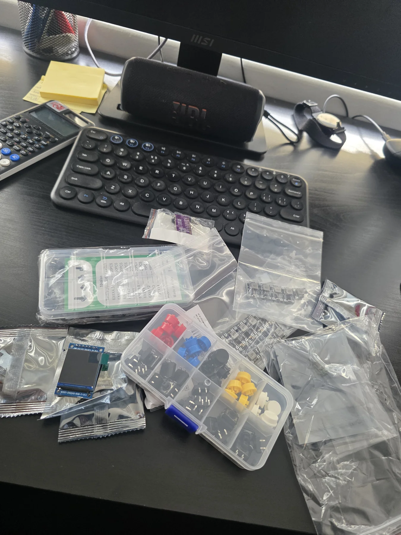
Phase 1 — Component Sourcing
ST7789 display, MicroSD breakout, tactile buttons, power modules
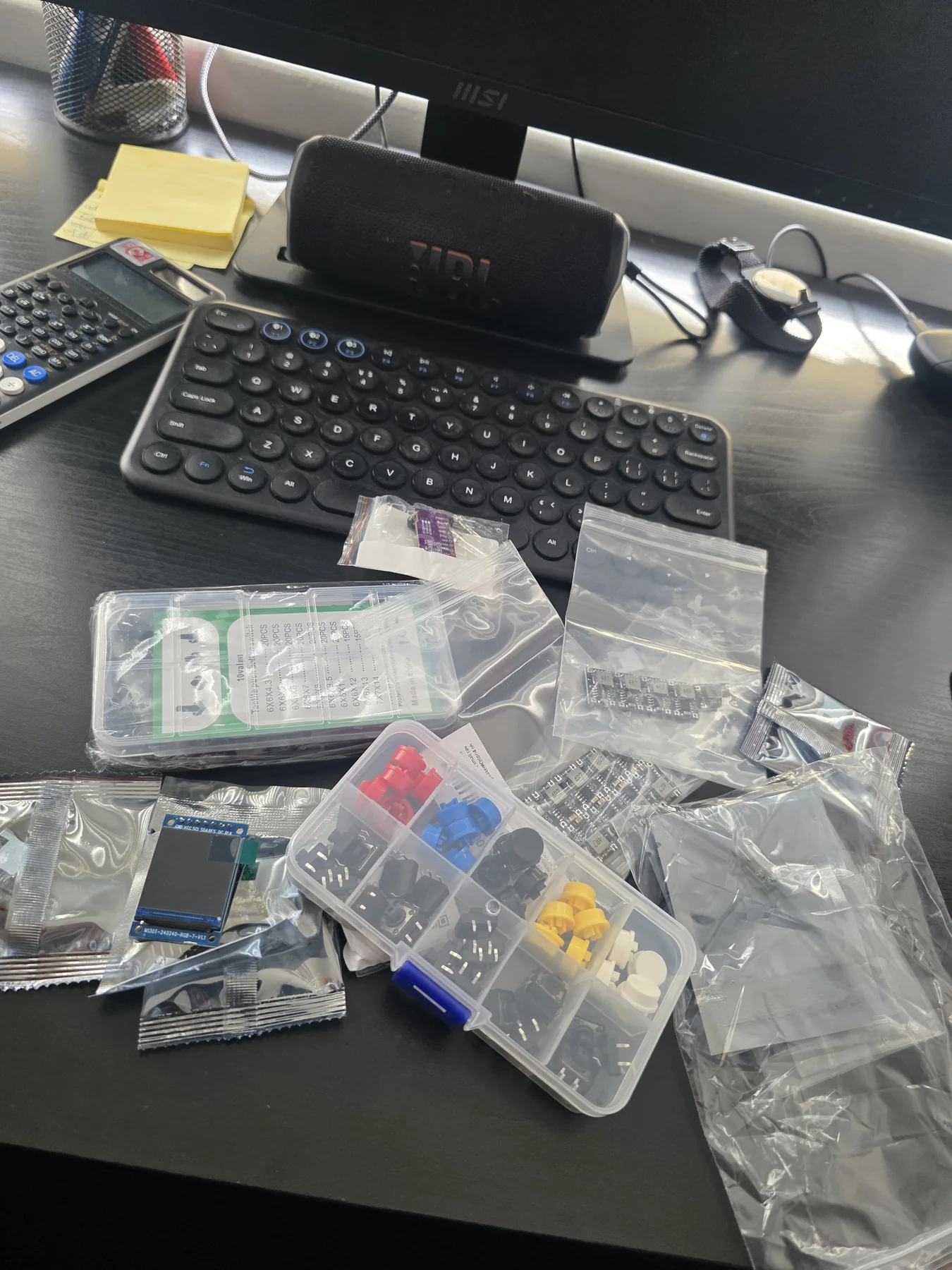
Sourced all modules independently: ST7789 1.3″ IPS TFT, MicroSD breakout, 8× tactile push buttons, IP5306 power bank IC, TP4056 USB-C charge module, and a LiPo cell. Each component was bench-tested for correct voltage and pin continuity before integration.
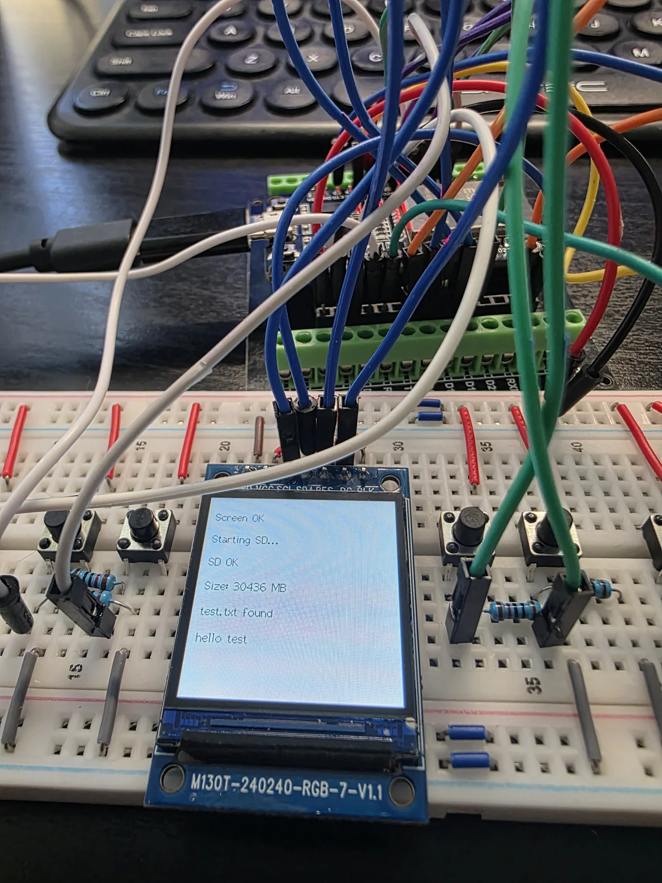
Phase 2 — Breadboard Prototype
First boot — display active, SD card detected, all subsystems validated
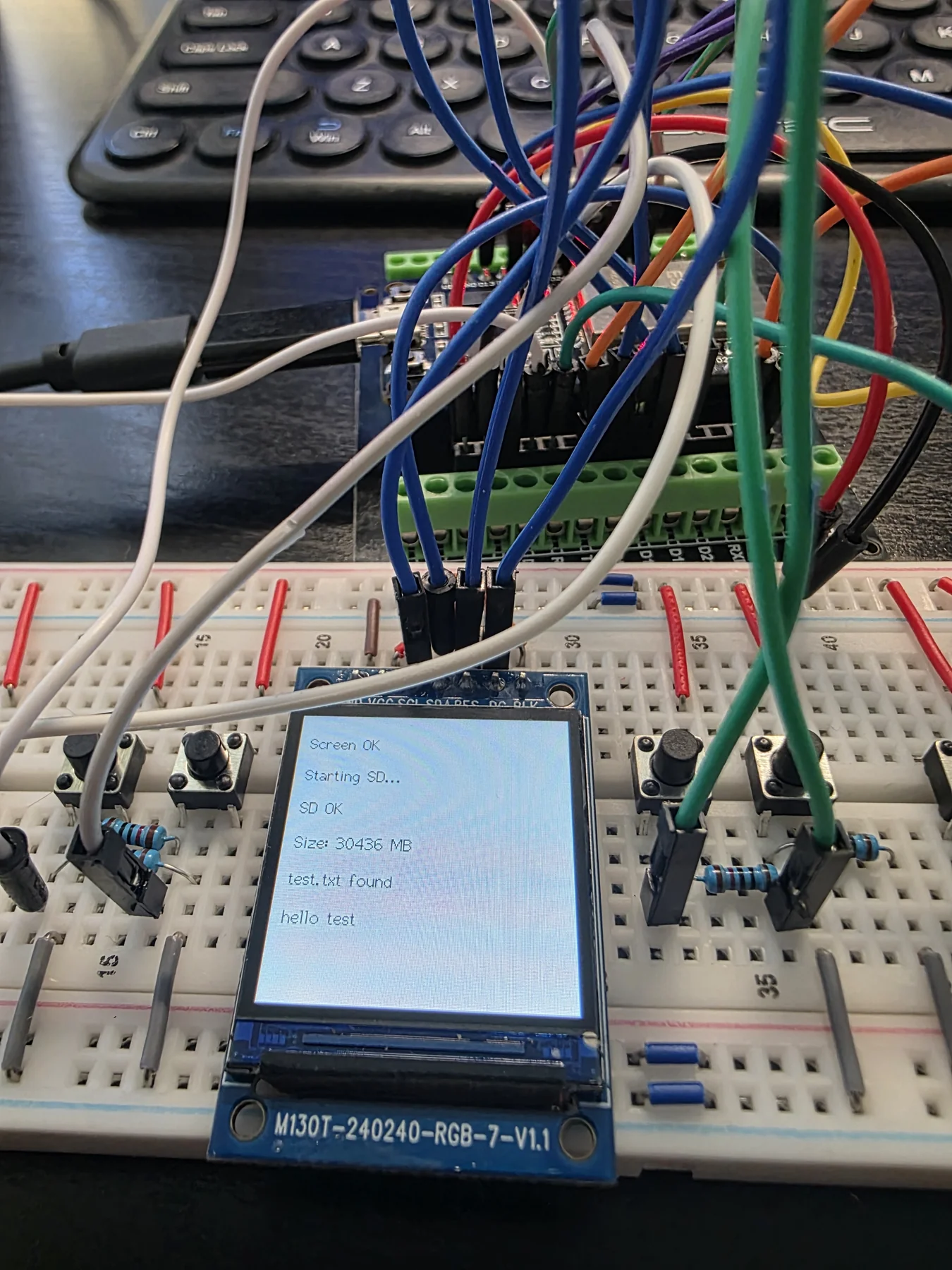
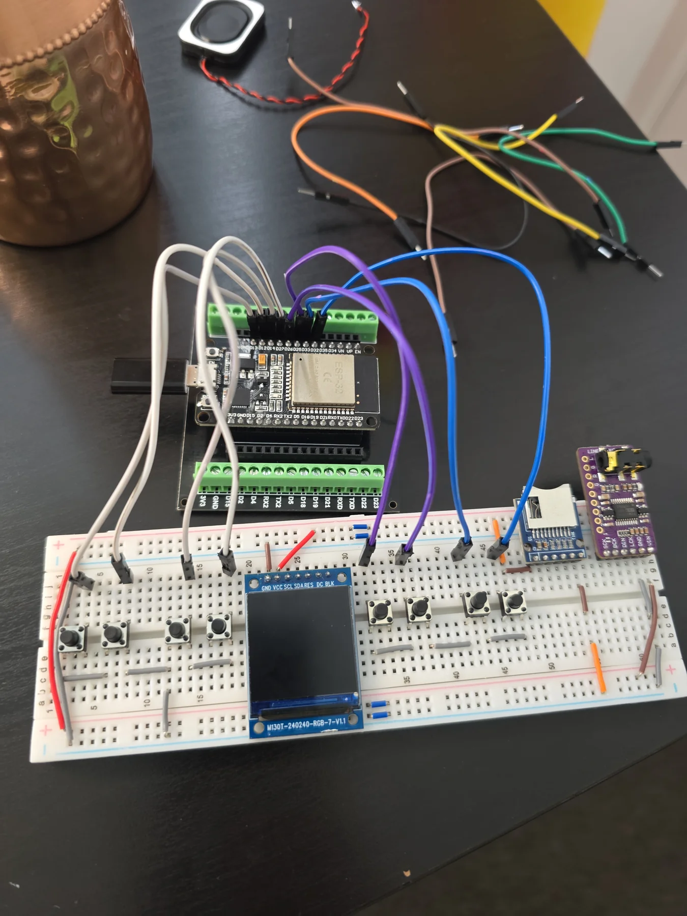
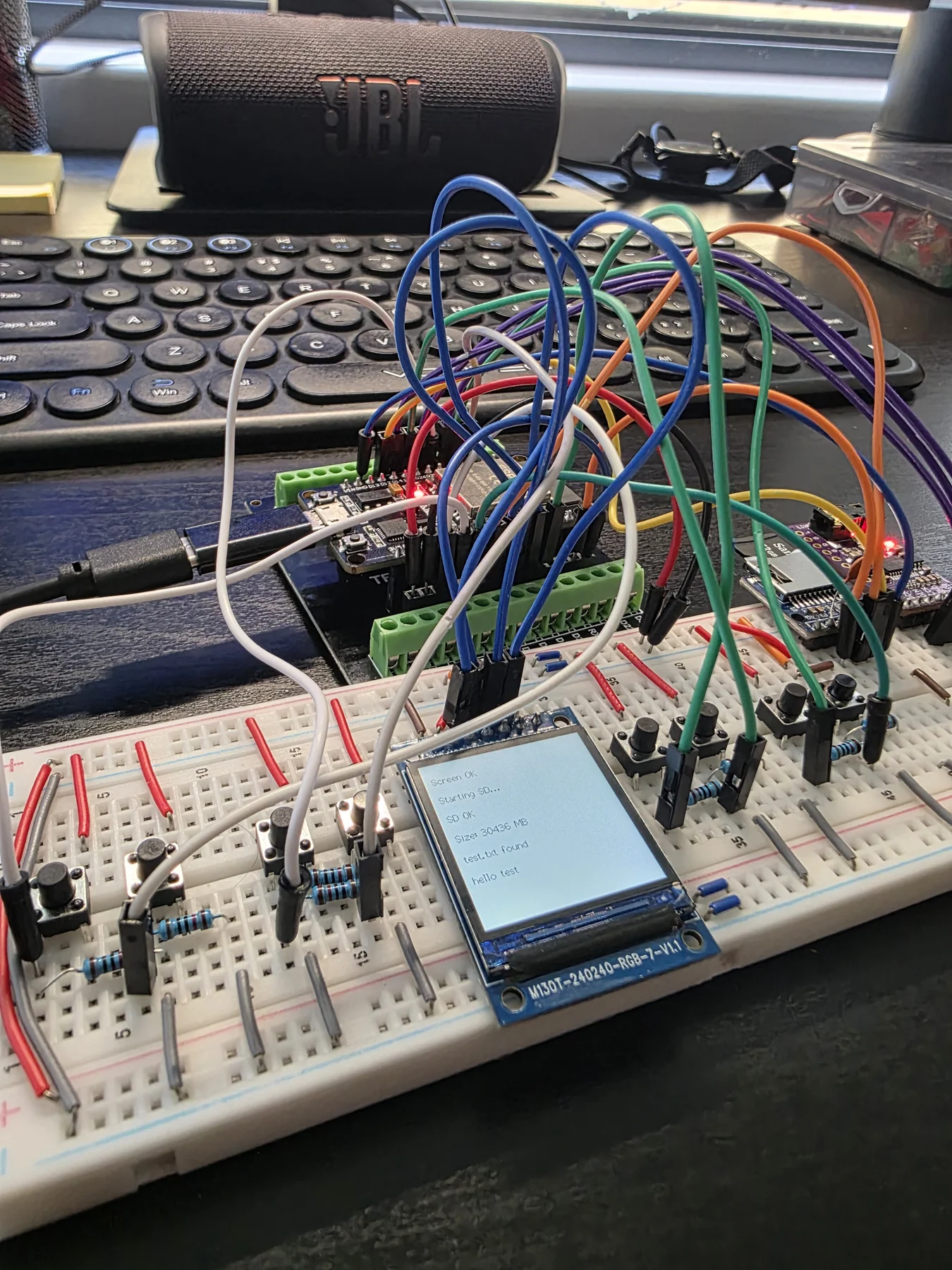
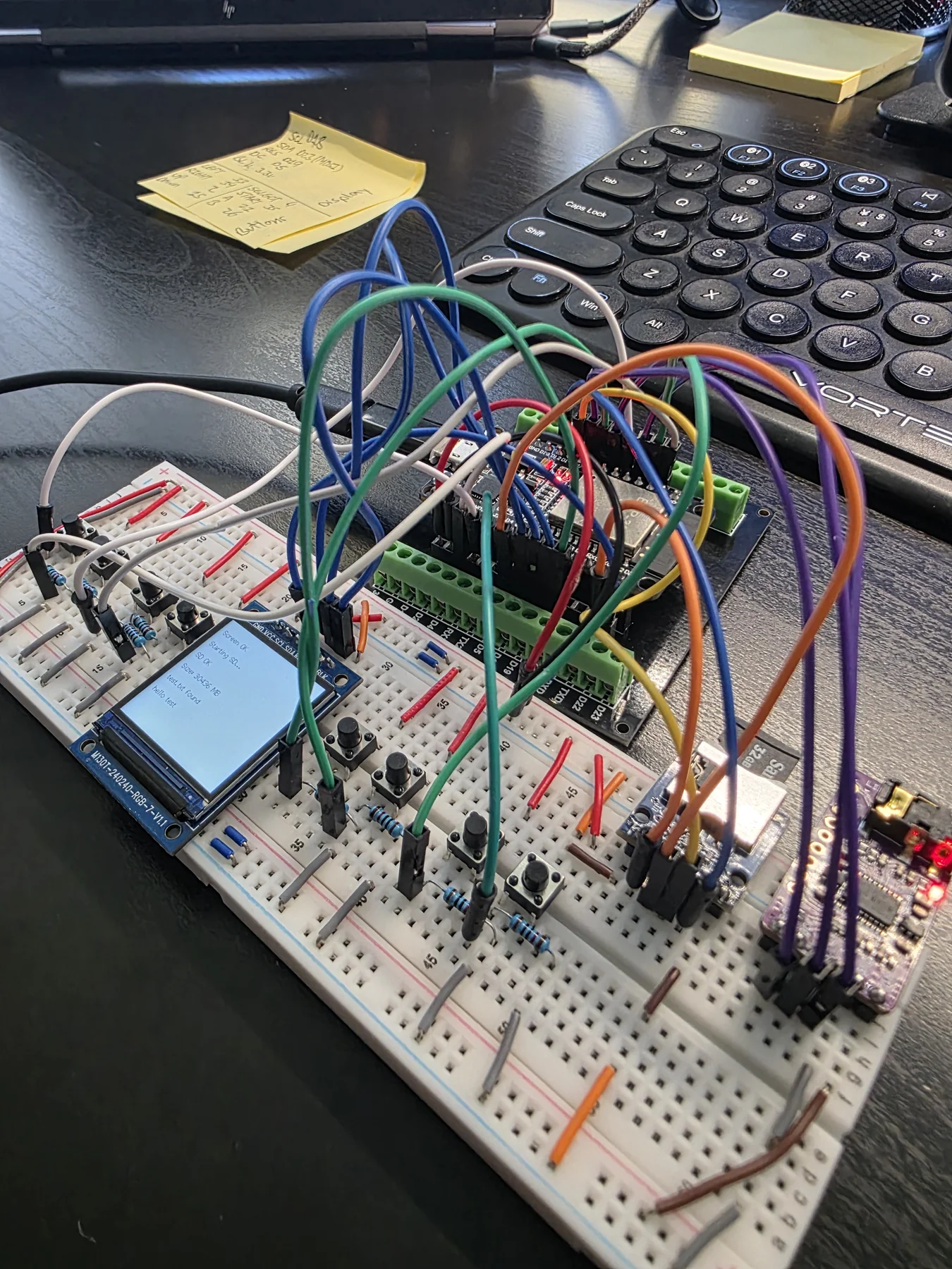
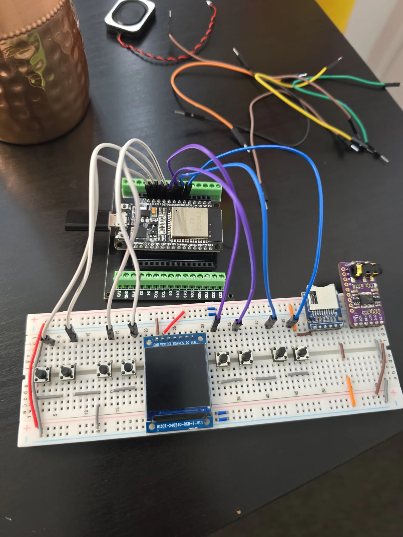
Built the first prototype on breadboard with all five subsystems. Achieved first boot with the display showing test output and the SD card detected at 30 GB. Button GPIO reads verified via serial monitor. The SPI bus conflict between display and SD was identified and resolved at this stage by moving SD to software SPI.
Phase 3 — Perfboard Assembly & Soldering
Hand-soldered front and back boards with colour-coded wiring harness
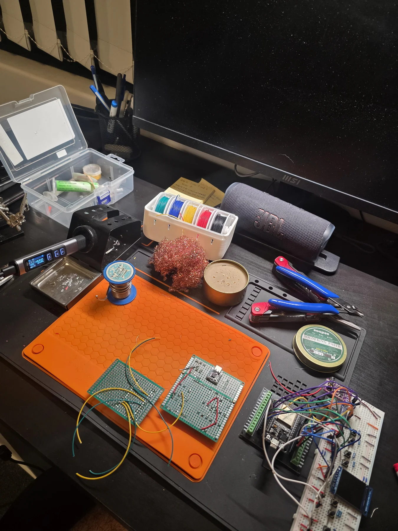
Components transferred from breadboard to perfboard using a temperature-controlled soldering station with paste flux. The front panel board carries the ST7789 display, D-pad, and A/B/Start/Select buttons. The back board carries the ESP32, MicroSD breakout, and IP5306 power IC. A colour-coded wiring harness connects the two boards for easy debugging.
Phase 4 — Power Integration & Final Testing
LiPo cell integrated with USB-C charge, 5 V boost, and 3.3 V logic rail
Integrated the LiPo 3.7 V cell with TP4056 USB-C charge IC and IP5306 5 V boost converter. Logic regulated to 3.3 V across all digital subsystems. Full NES ROM loading from MicroSD confirmed working. Display rendering verified across multiple games. With all subsystems running reliably, the prototype was complete.
07

Engineering Challenges

SPI Bus Conflict — Display vs MicroSD
Both the ST7789 display and MicroSD module use SPI. With TFT_CS set to –1, the display holds the hardware SPI bus permanently. Moving the SD card to software SPI (bit-banged) on dedicated pins (MOSI 17 · MISO 13 · SCK 14) freed the hardware bus exclusively for the display at 27 MHz, with no arbitration overhead or frame rate penalty.
I2S Audio — Designed Around CPU Load
Audio was not wired in the prototype, but the firmware was designed carefully for the PCB build. Simulation showed the 6502 emulation loop could cause buffer underruns. The fix: pre-fill the I2S DMA ring buffer at startup and run the audio task at higher FreeRTOS priority than the PPU renderer — so the buffer never runs dry regardless of emulation load.
GPIO Input Noise on Floating Button Lines
Floating GPIO inputs caused spurious button presses during testing. Fixed by enabling internal GPIO pull-up resistors and debouncing button reads across consecutive emulation frames — no external hardware required, and no interrupt-driven edge detection needed.
ROM Size Exceeds Available DRAM
ROMs larger than available DRAM cannot be copied into RAM. Solved using the spi_flash_mmap API to memory-map ROM data directly from SPI flash starting at address 0x00300000. The emulator accesses ROM as a const uint8_t* pointer without occupying any DRAM, enabling support for ROMs up to 512 kB.
08

PCB — Shipped as RetroDS v2

With the perfboard prototype validated, the next step was a custom 4-layer PCB in KiCad — a dedicated ground plane, separated analogue and digital ground zones for cleaner audio, and a single compact board replacing the two-board perfboard stack. The PCB design also upgraded the microcontroller to the ESP32-S3-WROOM-1U — adding native USB, 8 MB flash, and improved performance for emulation and audio. That board is built, brought up, and working — see RetroDS v2 for the full PCB design, the fault-finding session that got it running, and the firmware rewrite that added sound, volume control, save games, and an on-screen game-select menu.

Component Upgrades — Prototype → PCB
A few components were upgraded or swapped for the PCB build:

Microcontroller: ESP32-WROOM-32E → ESP32-S3-WROOM-1U. The S3 has native USB (connects directly to the USB-C port — no extra chip needed), 8 MB of flash (this N8 module has no PSRAM), and a faster processor.

Audio: No audio in the prototype. The PCB adds a MAX98357A — a single chip that handles both digital-to-analog conversion and amplification, driving a speaker directly from the I2S bus, with a 15-step volume control.

Power management: The prototype used two off-the-shelf breakout modules (IP5306 boost converter + TP4056 charger). The PCB replaces these with dedicated ICs: MCP73871 (proper LiPo charger with charge status outputs) and AP2112K (clean 3.3 V regulator).

USB protection: Added PRTR5V0U2X ESD protection on the USB data lines — important for a finished PCB connected to real USB ports.

SD card bus: The prototype bit-banged a software SPI to avoid sharing the hardware bus with the display. The PCB has two dedicated hardware SPI buses — one for the display, one for the SD card — no workaround needed.
3D-Printed Enclosure — Fusion 360
A snap-fit shell designed in Fusion 360 around the final PCB footprint. Features a screen cutout, button holes aligned to D-pad and action buttons, USB-C port access, and a speaker outlet. Printed in PLA on a Creality Ender-3 S1 Pro. Finished and fitted on RetroDS v2.

View implementation details — display config, pin defines, ROM loading, and audio setup

09

Demo

Gameplay — prototype running a ROM
Extended session — display and controls
← Mini RC Car ⌂ Portfolio RetroDS v2 — Custom PCB →
CODE NOTES — RetroDS

TFT_eSPI User_Setup.h

Edit this file in your Arduino libraries folder: Arduino\libraries\TFT_eSPI\User_Setup.h
Comment out ALL existing content, then paste the config below and save.

#define ST7789_DRIVER

#define TFT_WIDTH   240
#define TFT_HEIGHT  240

#define TFT_MOSI   23      // SPI Data
#define TFT_SCLK   18      // SPI Clock
#define TFT_DC      5      // Data / Command
#define TFT_RST    19      // Reset
#define TFT_CS     -1      // CS always active (display-only SPI bus)

#define SPI_FREQUENCY  27000000

#define LOAD_GLCD
#define LOAD_FONT2
#define LOAD_FONT4
#define LOAD_FONT6
#define LOAD_FONT7
#define LOAD_FONT8
#define LOAD_GFXFF

GPIO & I2S Pin Definitions

All pin assignments from NesCat.ino

// Buttons
#define PIN_UP      2
#define PIN_DOWN   15
#define PIN_LEFT   33
#define PIN_RIGHT  34
#define PIN_A      21
#define PIN_B      26
#define PIN_START  35
#define PIN_SELECT  4

// I2S Audio — MAX98357A (PCB build, not in prototype)
#define I2S_BCK_IO 27    // Bit Clock
#define I2S_WS_IO  32    // Word Select (LRC)
#define I2S_DO_IO  25    // Data Out

// MicroSD — Software SPI
#define SOFTSD_MOSI_PIN 17
#define SOFTSD_MISO_PIN 13
#define SOFTSD_SCK_PIN  14
#define SD_CS_PIN       22

ROM Loading — SPI Flash Memory Mapping

ROM is loaded from MicroSD into SPI flash at 0x00300000, then memory-mapped. The emulator accesses ROM data as a normal pointer without using any DRAM.

#define ROM_FLASH_ADDR   0x00300000
#define ROM_SECTOR_SIZE  0x1000     // 4 kB sectors

// After writing ROM bytes to flash:
const void *romPtr = nullptr;
spi_flash_mmap_handle_t mmapHandle;

esp_err_t err = spi_flash_mmap(
  ROM_FLASH_ADDR,
  romSizeAligned,
  SPI_FLASH_MMAP_DATA,
  &romPtr,
  &mmapHandle
);

// ROM now accessible as:
// const uint8_t* rom = (const uint8_t*)romPtr;
// No DRAM consumed — reads directly from flash mapping

I2S Audio Configuration

I2S driver config for the PCB build — not wired in the prototype. Drives the MAX98357A Class D amplifier at 16-bit stereo, 24 kHz. DMA ring buffer keeps audio smooth regardless of emulation CPU load.

#define DEFAULT_SAMPLERATE  24000
#define DEFAULT_FRAGSIZE    240   // Samples per DMA buffer

i2s_config_t i2s_config = {
  .mode             = I2S_MODE_MASTER | I2S_MODE_TX,
  .sample_rate      = DEFAULT_SAMPLERATE,
  .bits_per_sample  = I2S_BITS_PER_SAMPLE_16BIT,
  .channel_format   = I2S_CHANNEL_FMT_RIGHT_LEFT,
  .communication_format = I2S_COMM_FORMAT_PCM,
  .dma_buf_count    = 6,
  .dma_buf_len      = 4 * DEFAULT_FRAGSIZE,
  .use_apll         = false,
  .intr_alloc_flags = ESP_INTR_FLAG_LEVEL1
};

i2s_pin_config_t pin_config = {
  .bck_io_num    = I2S_BCK_IO,   // GPIO 27
  .ws_io_num     = I2S_WS_IO,    // GPIO 32
  .data_out_num  = I2S_DO_IO,    // GPIO 25
  .data_in_num   = I2S_PIN_NO_CHANGE
};
Click to swap image